
blind vias in HDI printed circuit boards
In PCBs, blind vias are holes drilled through layers without being connected to the copper-connecting pads on adjacent layers. These holes can reduce signal interference, noise, and distortion between the layers of the circuit board. They can also make it easier to route high-speed signals over the circuit board. Blind vias are often used in multilayer printed circuit boards, especially those that require high-density interconnect (HDI). They can be expensive to produce, but their benefits in demanding applications may outweigh the cost.
There are two different ways to produce blind vias in a hdi printed circuit board. The first is to use an eximer laser, which can drill through both the copper layer and underlying dielectric material at once. However, the laser must be carefully calibrated to avoid drilling through the copper-connecting pad on the next layer down.
The second way to produce blind vias is to drill them before the multilayer lamination process. This method is more expensive than the eximer laser method, but it can be cost-effective when there are a large number of them on a PCB.
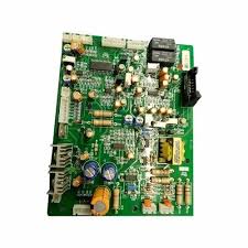
What are blind vias in HDI printed circuit boards?
Once the blind vias are drilled, they must be filled with copper to ensure that they will make good connections with the copper-connecting pads on each layer of the circuit board. The hole must be plated to the same level as the copper on that layer, which is sometimes called “buttoned plating.” This process can result in air bubbles forming underneath the solder balls in the holes.
When this occurs, the solder balls will not be able to contact each other, and the circuit board may not work properly. This can be resolved by placing the vias in such a position that they are not directly underneath the solder balls, or by using a build-up process to fill the holes with copper.
There are many other factors that can affect the quality of a PCB with blind vias, including the type of via used, its diameter and depth, the ratio of the hole height to the via diameter, and the size of the dielectric gap between layers. It is important to take all of these factors into account when designing a circuit board with blind vias.
In conclusion, HDI printed circuit boards are a pivotal technology in the advancement of modern electronics. Their ability to provide higher wiring density, support complex interconnections, and enable miniaturization makes them indispensable in a wide range of applications, from consumer electronics to medical devices and military systems. As electronic devices continue to evolve, the demand for HDI PCBs is likely to grow, driving further innovations in PCB design and manufacturing. The future of electronics will undoubtedly be shaped by the capabilities and advancements of HDI technology.
In addition to their use in HDI printed circuit boards, blind vias are an essential component of PCBs used in demanding applications such as mobile devices and high-speed digital circuits. They can help to improve signal performance and increase the density of the circuit board, and can even lower the overall layer count. Nevertheless, they can be difficult to manufacture and require meticulous planning. They can also introduce issues such as spacing problems and layer-count restrictions.


