
make a PCB prototype at home
Yes, it is possible to make a PCB prototype at home, and many hobbyists and electronics enthusiasts take on this challenge to create custom PCBs for their projects. While professional PCB manufacturing services offer advanced tools and a higher level of precision, home-based prototyping can be a cost-effective and educational way to create a PCB prototype for simpler designs. In this article, we will explore the process of making a PCB prototype at home, the tools you’ll need, and the advantages and challenges of this approach.
To begin creating a PCB prototype at home, you need the right tools and materials. The basic equipment includes a computer with PCB design software, a copper-clad board, a laser printer (for printing the PCB design onto paper), and either an etching solution or a CNC machine for engraving the PCB traces. The process starts with designing the PCB using design software like KiCad, Eagle, or EasyEDA. Once you have created your design, you will generate the necessary files, typically in Gerber format, and print the design onto a transparent film or paper. This printed design serves as the mask that will guide the etching process.
One of the most common methods for creating a pcb prototype at home is the toner transfer method. This process involves printing the PCB design onto a special transfer paper using a laser printer. After printing, the paper is placed onto the copper-clad board and heated, which causes the toner to transfer onto the board. Once the toner is in place, the board is immersed in an etching solution, such as ferric chloride or ammonium persulfate, which dissolves the exposed copper, leaving behind the PCB traces protected by the toner. This method is relatively simple and inexpensive but requires precision to ensure the toner adheres properly and that the etching process is uniform.
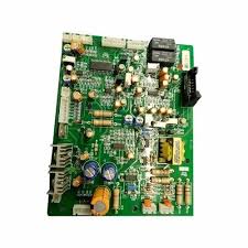
Can I make a PCB prototype at home?
Another approach for home-based PCB prototyping is using a CNC mill or a PCB milling machine. These machines use a rotating cutting tool to remove copper from the PCB, leaving behind the desired traces. CNC milling provides more precision than the toner transfer method and is often preferred for more complex designs or when higher levels of accuracy are required. However, the cost of purchasing or building a CNC milling machine can be significant, and it requires a certain level of expertise to operate. Milling also eliminates the need for chemical etching, which some people prefer due to environmental or safety concerns associated with the chemicals used in etching solutions.
For both methods, once the traces have been etched, the next step is drilling the holes for the components. Drilling can be done manually using a small handheld drill or using a CNC machine. After drilling, the board needs to be cleaned and the components soldered onto the PCB prototype. This step can be done using a soldering iron for through-hole components or a reflow oven for surface-mount components. Soldering requires a steady hand and patience, as the small components need to be placed accurately on the PCB.
While making a PCB prototype at home is achievable, it does come with its own set of challenges. The quality of the PCB prototype produced at home may not match the precision or reliability of professionally manufactured boards, especially when it comes to multi-layer designs or very fine traces. Additionally, the time and effort required for etching, drilling, and soldering can be quite extensive, particularly for complex circuits. Environmental concerns also come into play, as chemical etching solutions need to be disposed of properly to avoid pollution. Furthermore, while it is possible to produce one or two prototypes at home, mass production or large-scale prototypes would be impractical due to the time and resources involved.
In conclusion, making a PCB prototype at home is a viable option for those with the right tools and knowledge, particularly for simple circuits or small-scale projects. Techniques like toner transfer or CNC milling can be used to etch the copper traces, and basic soldering techniques can be applied for component assembly. However, for more advanced or larger-scale projects, professional PCB manufacturers are typically the better option due to their expertise, higher precision, and access to advanced equipment. Home-based prototyping is a great learning experience and offers a low-cost alternative for developing custom PCB prototypes for personal or educational use.


