
Rigid Flex PCB Manufacturer Process
The rigid flex pcb manufacturer process combines rigid and flexible circuit board manufacturing technologies to create boards that can be folded or twisted to fit your product’s shape. Rigid flex PCBs can help reduce space and weight requirements, while maintaining electrical integrity and signal routing. They are available in a wide range of sizes and thicknesses to suit your specific design needs.
The first step in the rigid flex pcb fabrication process is to prepare the base material. This involves cleaning or prepping the laminate containing copper layers and/or adhesives. Then, the printed circuit pattern is created using either screen printing or photo imaging techniques. Once the pattern is set, the etching process begins. The copper layer is etched by dipping or spraying an etchant solution onto the surface of the laminate. The copper is then plated through the etched holes to establish electrical connections between the rigid and flex sections of the board.
Next, the rigid section is routed with the appropriate pads and vias to connect the circuit to the flex sections of the PCB. The routing process also includes adding thermal and mechanical stiffeners to the rigid sections of the PCB. These stiffeners relieve strain, balance weight and heat dissipation, and increase abrasion resistance. They can also help prevent vibrations or bending in the boards that might cause signal degradation.
Rigid flex PCBs have very dense interconnections between the rigid and flex sections of the circuit board. This is achieved through a combination of drilling technology, desmear technology and electroless copper plating. The drilling process generates resin smear and debris that can stick to the hole walls, resulting in poor reliability. The smear can be removed by using chemical desmear like potassium permanganate. However, the use of this method can induce high-temperatures that may damage the rigid flex pcb material.
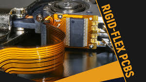
The 3 Steps in the Rigid Flex PCB Manufacturer Process
A specialized coverlay or solder mask is applied to the top and bottom surfaces of the flex area to protect the circuit from harsh weather conditions, chemicals, and solvents. This is an important step for ensuring a long life and high reliability of the flex circuit. Alternatively, an adhesive-less process is available where a photo-imageable solder mask is imprinted directly on the flex. The coverlay is then cured with UV exposure.
Lastly, the rigid flex pcb is cut out from the underlying production panel using a hydraulic punching tool or by hand with a specialized blanking knife for prototyping and small production runs. The flex circuit is then attached to the rigid section of the PCB using acrylic or epoxy-based adhesives.
The final step is to perform electrical testing and verification of the flex circuits to ensure compliance with your design specifications. This includes testing for continuity, isolation and signal quality to detect potential defects before releasing the circuit for mass production. The flex circuits are also tested for flex durability and compliance with mechanical and environmental standards. This step is critical to ensuring on-time delivery and a high-quality rigid flex pcb.


